- 您现在的位置:买卖IC网 > Sheet目录364 > SST25VF020-20-4C-QAE-T (Microchip Technology)IC FLASH SER 2MB 20MHZ SPI 8WSON
�� �
�
�2� Mbit� SPI� Serial� Flash�
�A� Microchip� Technology� Company�
�SST25VF020�
�Not� Recommended� for� New� Designs�
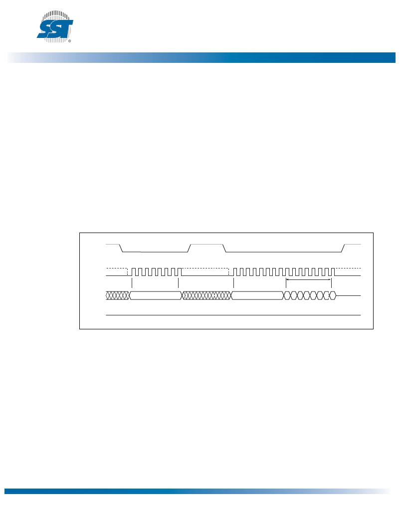
�Write-Status-Register� (WRSR)�
�The� Write-Status-Register� instruction� works� in� conjunction� with� the� Enable-Write-Status-Register�
�(EWSR)� instruction� to� write� new� values� to� the� BP1,� BP0,� and� BPL� bits� of� the� status� register.� The� Write-�
�Status-Register� instruction� must� be� executed� immediately� after� the� execution� of� the� Enable-Write-Sta-�
�tus-Register� instruction� (very� next� instruction� bus� cycle).� This� two-step� instruction� sequence� of� the�
�EWSR� instruction� followed� by� the� WRSR� instruction� works� like� SDP� (software� data� protection)� com-�
�mand� structure� which� prevents� any� accidental� alteration� of� the� status� register� values.� The� Write-Sta-�
�tus-Register� instruction� will� be� ignored� when� WP#� is� low� and� BPL� bit� is� set� to� “1”.� When� the� WP#� is�
�low,� the� BPL� bit� can� only� be� set� from� “0”� to� “1”� to� lock-down� the� status� register,� but� cannot� be� reset�
�from� “1”� to� “0”.� When� WP#� is� high,� the� lock-down� function� of� the� BPL� bit� is� disabled� and� the� BPL,� BP0,�
�and� BP1� bits� in� the� status� register� can� all� be� changed.� As� long� as� BPL� bit� is� set� to� 0� or� WP#� pin� is�
�driven� high� (V� IH� )� prior� to� the� low-to-high� transition� of� the� CE#� pin� at� the� end� of� the� WRSR� instruction,�
�the� BP0,� BP1,� and� BPL� bit� in� the� status� register� can� all� be� altered� by� the� WRSR� instruction.� In� this�
�case,� a� single� WRSR� instruction� can� set� the� BPL� bit� to� “1”� to� lock� down� the� status� register� as� well� as�
�altering� the� BP0� and� BP1� bit� at� the� same� time.� See� Table� 2� for� a� summary� description� of� WP#� and� BPL�
�functions.� CE#� must� be� driven� low� before� the� command� sequence� of� the� WRSR� instruction� is� entered�
�and� driven� high� before� the� WRSR� instruction� is� executed.� See� Figure� 14� for� EWSR� and� WRSR� instruc-�
�tion� sequences.�
�CE#�
�SCK�
�MODE� 3�
�MODE� 0�
�0� 1� 2� 3� 4� 5� 6� 7�
�MODE� 3�
�MODE� 0�
�0� 1� 2� 3� 4� 5� 6� 7� 8� 9� 10� 11� 12� 13� 14� 15�
�STATUS�
�REGISTER� IN�
�SI�
�SO�
�MSB�
�50�
�01�
�MSB�
�HIGH� IMPEDANCE�
�7� 6� 5� 4� 3� 2� 1� 0�
�MSB�
�1231� F13.1�
�Figure� 14:� Enable-Write-Status-Register� (EWSR)� and� Write-Status-Register� (WRSR)�
�Sequence�
�?2011� Silicon� Storage� Technology,� Inc.�
�16�
�DS25078A�
�11/11�
�发布紧急采购,3分钟左右您将得到回复。
相关PDF资料
SST25VF020B-80-4C-QAE-T
IC FLASH SER 2MB 80MHZ SPI 8WSON
SST25VF032B-66-4I-S2AF
IC FLASH SER 32M 66MHZ SPI 8SOIC
SST25VF040B-50-4C-ZAE
IC FLASH SER 4MB 80MHZ SPI 8CSP
SST25VF040B-80-4I-QAE
IC FLASH SER 4MB 80MHZ SPI 8WSON
SST25VF064C-80-4I-Q2AE-T
IC FLASH SER 64M DUAL I/O 8WSON
SST25VF080B-80-4I-QAE-T
IC FLASH SER 8MB 50MHZ SPI 8WSON
SST25VF512-20-4C-SAE-T
IC FLASH SER 512K 20MHZ 8SOIC
SST25VF512A-33-4I-QAE-T
IC FLASH SER 512KB 33MHZ 8WSON
相关代理商/技术参数
SST25VF020-20-4C-S2AE
制造商:SST 制造商全称:Silicon Storage Technology, Inc 功能描述:2 Mbit / 4 Mbit SPI Serial Flash
SST25VF020204CSA
制造商:Silicon Storage Technology (SST) 功能描述: 制造商:SST 功能描述:
SST25VF020-20-4C-SA
功能描述:闪存 256K X 8 14 us
RoHS:否 制造商:ON Semiconductor 数据总线宽度:1 bit 存储类型:Flash 存储容量:2 MB 结构:256 K x 8 定时类型: 接口类型:SPI 访问时间: 电源电压-最大:3.6 V 电源电压-最小:2.3 V 最大工作电流:15 mA 工作温度:- 40 C to + 85 C 安装风格:SMD/SMT 封装 / 箱体: 封装:Reel
SST25VF020-20-4C-SAE
功能描述:闪存 256K X 8 14 us RoHS:否 制造商:ON Semiconductor 数据总线宽度:1 bit 存储类型:Flash 存储容量:2 MB 结构:256 K x 8 定时类型: 接口类型:SPI 访问时间: 电源电压-最大:3.6 V 电源电压-最小:2.3 V 最大工作电流:15 mA 工作温度:- 40 C to + 85 C 安装风格:SMD/SMT 封装 / 箱体: 封装:Reel
SST25VF020-20-4C-SAE-T
功能描述:闪存 2M (256Kx8) 20MHz 2.7-3.6V Commercial RoHS:否 制造商:ON Semiconductor 数据总线宽度:1 bit 存储类型:Flash 存储容量:2 MB 结构:256 K x 8 定时类型: 接口类型:SPI 访问时间: 电源电压-最大:3.6 V 电源电压-最小:2.3 V 最大工作电流:15 mA 工作温度:- 40 C to + 85 C 安装风格:SMD/SMT 封装 / 箱体: 封装:Reel
SST25VF020-20-4E-QA
功能描述:闪存 256K X 8 14 us
RoHS:否 制造商:ON Semiconductor 数据总线宽度:1 bit 存储类型:Flash 存储容量:2 MB 结构:256 K x 8 定时类型: 接口类型:SPI 访问时间: 电源电压-最大:3.6 V 电源电压-最小:2.3 V 最大工作电流:15 mA 工作温度:- 40 C to + 85 C 安装风格:SMD/SMT 封装 / 箱体: 封装:Reel
SST25VF020-20-4E-QAE
功能描述:闪存 256K X 8 14 us
RoHS:否 制造商:ON Semiconductor 数据总线宽度:1 bit 存储类型:Flash 存储容量:2 MB 结构:256 K x 8 定时类型: 接口类型:SPI 访问时间: 电源电压-最大:3.6 V 电源电压-最小:2.3 V 最大工作电流:15 mA 工作温度:- 40 C to + 85 C 安装风格:SMD/SMT 封装 / 箱体: 封装:Reel
SST25VF020-20-4E-S2AE
制造商:SST 制造商全称:Silicon Storage Technology, Inc 功能描述:2 Mbit / 4 Mbit SPI Serial Flash